-40%
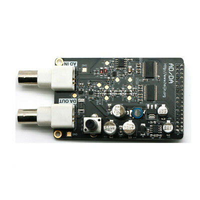
New High-speed AD9708 AD9280 AD / DA Module FPGA Development Board
$ 12.67
- Description
- Size Guide
Description
elecbuyHome
Description
Payment
Shipping
Terms of sale
About Us
New High-speed AD9708 AD9280 AD / DA Module FPGA Development Board
Features:
1
.
Digital to analog converter (DA) circuit
Such as hardware structure shown in the figure, the DA circuit is composed of a high speed DA chip, 7 Gai Butterworth low pass filter, amplitude
Regulating circuit and a signal output interface.
High speed DA chip we are using AD's AD9708. AD9708 is a 8 bit, 125MSPS
DA conversion chip, built-in 1.2V reference voltage, a differential current output. The internal structure of the chip diagram as shown below:
After the AD9708 chip differential output, in order to prevent noise interference, connected in the circuit of 7 Gai Ba Talwar Si low pass filter, the bandwidth of 40MHz, frequency response as shown below:
The filter parameters as shown below:
After the filters, we use 2 pieces of high performance 145MHz bandwidth operational amplifier AD8056, realize the difference Variational single ended, and amplitude adjustment and other functions, so that the whole circuit performance has been improved to the greatest extent. Range regulation, is using the 5K potentiometer, the range of output end is -5V~5V (10Vpp).
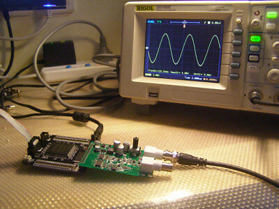
Waveform display:
2.Analog-to-digital converter (AD) circuit
As the hardware structure is shown in the picture, the AD circuit is composed of a high speed AD chip, attenuation circuit and a signal input interface Form. High speed AD chip we are using 8 developed by AD company, the maximum sampling rate of 32MSPS .AD9280 chip. The internal structure as shown below:
According to the following configuration, we will AD input voltage range is set to: 0V~2V:
Before the signal into the AD chip, we use a piece of AD8056 chip to construct the attenuation circuit, interface
The input range is -5V~+5V (10Vpp). Attenuation after, input range to meet the input range of the AD chip
(0~2V). The conversion formula is as follows:
When the input signal Vin=5 (V) time, signal input to the Vad=2 AD (V);
When the input signal Vin=-5 (V) time, signal input to the Vad=0 AD (V);kaPacakge
Package Contents
100% Brand New
1 x
High-speed AD9708 AD9280 AD / DA Module FPGA Development Board Black Gold
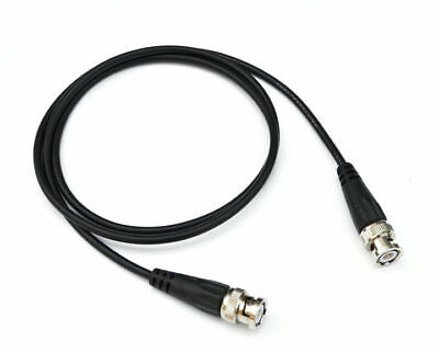
1 x BNC cable
Payment
We accept PayPal only.
Shipping
1.Items are shipped from china.we will send out within 1 bussiness day after receive the payment.
2.We only ship to ebay confirmed address. So before bidding, please kindly verify your ebay address.
3.
Shipping to USA takes 8-18 days in normal condition by E-packet with tracking number.
Shipping to most other countries takes about 12-30 days via Economy Int'l Airmail.
Less than , without free tracking number,if you request tracking number,please send ebay message to us.
Over ,with tracking number free.The shipping time depends on your location and local postal service,as well as the weather condition along the shipping,sometimes may take longer,.please send ebay message to us if you didn't get your package.
4.Express shipping: Extra -- will be charged for the first 500 grams for most countries. Send ebay message to us if you need this service.
Terms of sale
1.If you are not satisfied when you receive your item, please return it within 30 days for a replacement or money back. Please send ebay message to us before you return it.
2.If item is defective in 30 days, We will send you a replacement without extra charger, or offer refund after we receive the defective item.
3.If item is defective after 30 days, you can still send it back to us. We will send you a new one after receiving the defective item. But you have to pay the extra shipping fee.
About us
We are honest seller and do our best to serve you.
So if you have any concerns,please don’t hesitate to send ebay message to us.
